Home
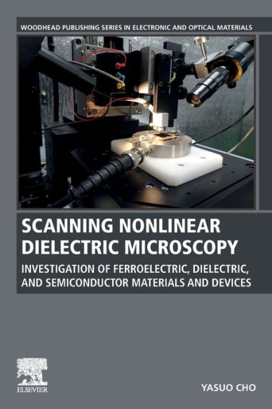
Scanning Nonlinear Dielectric Microscopy: Investigation of Ferroelectric, Dielectric, and Semiconductor Materials and Devices
Barnes and Noble
Scanning Nonlinear Dielectric Microscopy: Investigation of Ferroelectric, Dielectric, and Semiconductor Materials and Devices
Current price: $200.00


Barnes and Noble
Scanning Nonlinear Dielectric Microscopy: Investigation of Ferroelectric, Dielectric, and Semiconductor Materials and Devices
Current price: $200.00
Size: OS
Loading Inventory...
*Product information may vary - to confirm product availability, pricing, shipping and return information please contact Barnes and Noble
Scanning Nonlinear Dielectric Microscopy: Investigation of Ferroelectric, Dielectric, and Semiconductor Materials and Devices
is the definitive reference on an important tool to characterize ferroelectric, dielectric and semiconductor materials. Written by the inventor, the book reviews the methods for applying the technique to key materials applications, including the measurement of ferroelectric materials at the atomic scale and the visualization and measurement of semiconductor materials and devices at a high level of sensitivity. Finally, the book reviews new insights this technique has given to material and device physics in ferroelectric and semiconductor materials.
The book is appropriate for those involved in the development of ferroelectric, dielectric and semiconductor materials devices in academia and industry.


